Op-Amp: Input Bias Current and Input Offset Current Explained HD
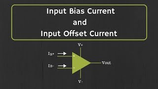
In this video, op-amp input bias current and input offset currents are explained. What is input bias current and input offset current? If op-amp is ideal then it is assumed that the no current is flowing into the input terminals of the op-amp. But actually when biasing voltages are applied to the op-amp then a small amount of current used to flow through these input terminals. And these currents are known as the input bias currents of the op-amp. In data sheets, it is defined as the average value of the input bias currents flowing in the two terminals of the op-amp. (Inverting and non-inverting terminal) Ideally both input bias currents (IB+ and IB-) should be identical, but actually, because of the slight mismatch between the two transistors of the differential amplifiers, these currents are slightly different. And the difference between the two input bias current is defined as the input offset current. The typical value of this input bias current for general purpose op-amp is few nanoamperes. But it can be as large as few micro-amperes for very high-speed op-amps and it can be as low as few pico-amperes for very high precision op-amps. Being very small current, the effect of this input bias current is negligible for most of the applications. But in the applications where a very precise output is required at that time this input bias current (and input offset voltage) becomes a very critical parameter. Input bias current compensation: By connecting the external offset compensation resistor at the non-inverting terminal the effect of input bias current can be minimized or removed. For compensation, the value of this compensation resistor should be equal to (R1 || Rf). Input offset current drift and input bias current drift with temperature: With temperature, the input bias current and input offset current used to get changed. The drift in these currents can be positive or negative. And in datasheets, it is defined in the unit of pA/C. The effect of the drift in this input offset current and input bias current is very small in the output offset voltage and most of the time it is negligible. By maintaining the ambient temperature around the circuit, the effect of this drift on the output error voltage can be reduced. The timestamps for the different topics covered in the video: 0:48 What is input bias current and input offset current? 6:08 Input bias current compensation using the offset compensation resistor 12:16 Example This video will be helpful to all students of science and engineering in understanding the input offset current and input bias current in the op-amp. Follow me on YouTube: https://www.youtube.com/allaboutelectronics Follow me on Facebook: https://www.facebook.com/ALLABOUTELECRONICS/ Follow me on Instagram: https://www.instagram.com/all_about.electronics/ Music Credit: http://www.bensound.com/
 HD
HD HD
HD HD
HD HD
HD HD
HD HD
HD HD
HD HD
HD HD
HD
 HD
HD
 HD
HD HD
HD
 HD
HD HD
HD HD
HD![DC Motor Driver using Power Mosfets [PWM Controlled, 30A Half Bridge]](https://i.ytimg.com/vi/9UVxvpHyqMI/mqdefault.jpg) HD
HD HD
HD HD
HD HD
HD HD
HD HD
HD
 HD
HD HD
HD HD
HD HD
HD HD
HD HD
HD HD
HD